Nanoimprint lithography

Nanoimprint lithography

Nanoimprint lithography is a low cost, high throughput and high resolution manufacturing process for nanoscale patterns, in which the nanoscale structures are formed by the mechanical deformation of a molten polymer and its subsequent cooling or of a monomer or prepolymer and its subsequent curing by temperature or by light.

TEKNIKER works with hot embossing/nanoimprint lithography which allows the structuring by both discontinuous and continuous methods of thermoplastic polymers either in bulk or deposited as a thin layer on a substrate, in this case allowing the replication of the original mould (master) or its inverse, by means of a combination with deposition and etching processes.

These processes make it possible to obtain resolutions in the range of the master employed, being able to achieve defined structures in the range of tens of nanometres.

Micro and nanostructured substrates manufactured using lithography can be used for a wide range of applications (optics and photonics, biotechnology, sensors, obtaining superhydrophobic surfaces, decorative finishes, anti-counterfeiting designs, etc.).

Related contents

  • Array ( [id] => 45 [idcategoria] => 2 [idsubcategoria] => 41 [imagen] => 01_AI_IS_NIL.jpg [caso_exito_1] => 2 [caso_exito_2] => 3 [caso_exito_3] => [cliente_1] => [cliente_2] => [cliente_3] => [direcciones_email] => consultasweb@tekniker.es [titulo] => Nanoimprint lithography [video] => [texto_1] =>

    Nanoimprint lithography is a low cost, high throughput and high resolution manufacturing process for nanoscale patterns, in which the nanoscale structures are formed by the mechanical deformation of a molten polymer and its subsequent cooling or of a monomer or prepolymer and its subsequent curing by temperature or by light.

    [fase_1] => [fase_2] => [fase_3] => [fase_4] => [texto_2] =>

    TEKNIKER works with hot embossing/nanoimprint lithography which allows the structuring by both discontinuous and continuous methods of thermoplastic polymers either in bulk or deposited as a thin layer on a substrate, in this case allowing the replication of the original mould (master) or its inverse, by means of a combination with deposition and etching processes.

    These processes make it possible to obtain resolutions in the range of the master employed, being able to achieve defined structures in the range of tens of nanometres.

    Micro and nanostructured substrates manufactured using lithography can be used for a wide range of applications (optics and photonics, biotechnology, sensors, obtaining superhydrophobic surfaces, decorative finishes, anti-counterfeiting designs, etc.).

    [texto_tabla] => [enlace_flickr] => https://www.flickr.com/photos/teknikerik4/sets/72157650235978597/ [enlace_youtube] => https://www.youtube.com/playlist?list=PLdI9ptv1PWExlEqTh50XRXuSQjQwTCj07 [enlace_issuu] => [enlace_slideshare] => [seo_h1] => Nanoimprint lithography [seo_url] => nanoimprint-lithography [seo_title] => Nanoimprint Lithography - TEKNIKER [seo_desc] => TEKNIKER works with hot embossing/nanoimprint lithography which allows the structuring by both discontinuous and continuous methods of thermoplastic polymers [imagenes] => [enlaces] => Array ( [0] => Array ( [imagen] => [titulo] => Paul Scherrer Institut [texto_corto] => [enlace] => http://www.psi.ch/ [alt] => Paul Scherrer Institut ) [1] => Array ( [imagen] => [titulo] => 3B’s Research Group [texto_corto] => [enlace] => http://www.3bs.uminho.pt/ [alt] => 3B’s Research Group ) [2] => Array ( [imagen] => [titulo] => Institut Català de Nanociència i Nanotecnologia [texto_corto] => [enlace] => https://icn2.cat/en/ [alt] => Institut Català de Nanociència i Nanotecnologia ) [3] => Array ( [imagen] => [titulo] => Denmarks Tekniske Universitet [texto_corto] => [enlace] => http://www.dtu.dk/english [alt] => Denmarks Tekniske Universitet ) [4] => Array ( [imagen] => [titulo] => Instituto de Microelectrónica de Barcelona [texto_corto] => [enlace] => http://www.imb-cnm.csic.es/index.php/en/ [alt] => Instituto de Microelectrónica de Barcelona ) [5] => Array ( [imagen] => [titulo] => Centro Nacional de Microelectrónica - Madrid [texto_corto] => [enlace] => http://www.imm.cnm.csic.es/es [alt] => Centro Nacional de Microelectrónica - Madrid ) [6] => Array ( [imagen] => [titulo] => Innovent [texto_corto] => [enlace] => http://www.innovent-jena.de/en/site__2/ [alt] => Innovent ) [7] => Array ( [imagen] => [titulo] => Biomedical Materials Group, Martin Luther Universität Halle-Wittenberg [texto_corto] => [enlace] => http://bmm.pharmazie.uni-halle.de/?lang=en [alt] => Biomedical Materials Group, Martin Luther Universität Halle-Wittenberg ) [8] => Array ( [imagen] => [titulo] => Departamento de Física Aplicada, Universidad de Alicante [texto_corto] => [enlace] => http://dfapl.ua.es/es/ [alt] => Departamento de Física Aplicada, Universidad de Alicante ) [9] => Array ( [imagen] => [titulo] => Fagor Automation [texto_corto] => [enlace] => http://www.fagorautomation.com/ [alt] => Fagor Automation ) [10] => Array ( [imagen] => [titulo] => Grupo Tirso [texto_corto] => [enlace] => http://www.tirso.org/ [alt] => Grupo Tirso ) [11] => Array ( [imagen] => [titulo] => Histocell [texto_corto] => [enlace] => http://www.histocell.com/index.php/en/ [alt] => Histocell ) [12] => Array ( [imagen] => [titulo] => Proteomika [texto_corto] => [enlace] => http://www.proteomika.com/ [alt] => Proteomika ) ) [publicaciones] => Array ( [0] => Array ( [titulo] => Artificial dermis, artificial skin, methods for their preparation and their uses [enlace] => en/inventions#P131577ES ) [1] => Array ( [titulo] => Biosensing for disease monitoring: metallic nanohole array plasmonic sensors based on scalable nanofabrication techniques [enlace] => biosensing-for-disease-monitoring-metallic-nanohole-array-plasmonic-sensors-based-on-scalable-nanofabrication-techniques ) [2] => Array ( [titulo] => Preliminary study on different technological tools and polymeric materials towards superhydrophobic surfaces for automotive applications [enlace] => preliminary-study-on-different-technological-tools-and-polymeric-materials-towards-superhydrophobic-surfaces-for-automotive-applications ) [3] => Array ( [titulo] => Surface microstructuring and protein patterning using hyaluronan derivatives [enlace] => surface-microstructuring-and-protein-patterning-using-hyaluronan-derivatives ) [4] => Array ( [titulo] => Protein patterning on the micro- and nanoscale by thermal nanoimprint lithography on a new functionalized copolymer [enlace] => protein-patterning-on-the-micro-and-nanoscale-by-thermal-nanoimprint-lithography-on-a-new-functionalized-copolymer ) [5] => Array ( [titulo] => Protein patterning by thermal nanoimprint lithography and NH3-plasma functionalization of polystyrene [enlace] => protein-patterning-by-thermal-nanoimprint-lithography-and-nh3-plasma-functionalization-of-polystyrene ) ) [sectores] => Array ( [0] => Array ( [titulo] => Automotive [seo_url] => automotive [imagen] => automocion.svg ) [1] => Array ( [titulo] => Renewable energy [seo_url] => renewable-energy [imagen] => energias_renovables.svg ) ) [soluciones] => Array ( [0] => Array ( [titulo] => Sensor devices [seo_url] => sensor-devices [imagen] => ST_DispositivosSensores_808x450px_icono.jpg ) [1] => Array ( [titulo] => Inspection and measuring [seo_url] => inspection-and-measuring [imagen] => ST_InspeccionMedida_808x450px_icono.jpg ) [2] => Array ( [titulo] => Multifunctional surfaces [seo_url] => multifunctional-surfaces [imagen] => ST_SuperficiesMultifuncionales_808x450px_icono.jpg ) ) [equipamiento] => Array ( [0] => Array ( [id] => 2 [titulo] => 
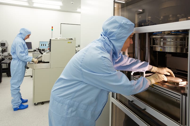
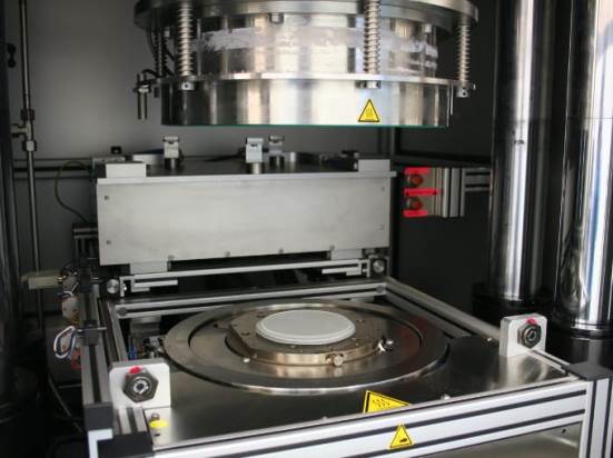
Jenoptik HEX 03 hot embossing/lithography nanoimprint system [imagen] => Sistema_Estampado_Caliente_Litrografia_Nanoimpresion.jpg [texto] =>
    CHARACTERISTICS OF THE EQUIPMENT
    • Maximum temperature of 220ºC
    • Maximum force of 200 kN
    • Prepared for working with moulds of up to 4 inches

    EXPERTISE

    • Fast manufacture of polymeric prototypes
    • Manufacture of sensors and biosensors
    • Manufacture of biodevices
    • Manufacture of photonic/optical devices
    • Obtaining surfaces with functional features arising from its topography (anti-reflecting, controlled hydrophilia/hydrophobia, protein adhesion or repulsion with influence on cell behaviour, etc.)
    ) [1] => Array ( [id] => 103 [titulo] => 
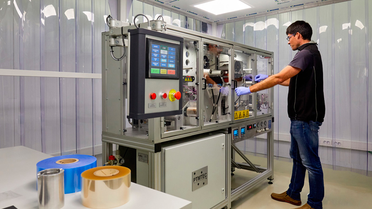
Continuous stamping system with nanoimprinting lithography [imagen] => IMG_Roll_to_Roll_767x431.jpg [texto] =>

    CHARACTERISTICS OF THE UNIT

    • Ultraviolet (UV) curing and thermal heating modules
    • Velocity range: 0.05-5 m/min
    • Resin deposit by reverse gravure coating
    • Maximum pressure of the thermal module: 5000 N
    • Temperature up to 250ºC
    • Film width of 100 mm
    • Ultrasound alignment of the film
    • Process tension sensor

    EXPERTISE

    • Obtaining surfaces with functional characteristics due to their topography (anti-reflection, controlled hydrophilia/hydrophobia, with influence on cell behaviour, anti-counterfeiting, decorative, etc.).
    ) ) )

Industrial sectors