
Validation of optical measurement technologies
TEKNIKER is carrying out research based on the micro and nanostructuring of components focused on applications in diverse fields, such as optical linear and angle encoders or label-free photonic biosensors.
The label-free photonic biosensors developed are based on two separate principles, although both are linked to the presence of nanostructures. Thus, biosensors based on both DFB lasers (Distributed Feedback) and on LSPR (Localised Surface Plasmon Resonance) have been developed.
These sensors are minimally invasive, given that markers for detecting a biomolecule in question (biomarkers) are not necessary. Moreover, the quantity of sample required for its detection is very small.
In both cases, both DFB lasers and LSPR, in order to ensure the sensing of the target biomolecule and not of any other that may be present in the sample, the nanostructured surfaces are biofuntionalize with the specific antibody for the biomarker.
The main developments currently being undertaken are focused on biomedicine and optical biosensors, but these devices can be adapted to the quality control for lubricating oils, for the automobile and the machine tools sectors, as well as in aeronautics.
Industrial sectors


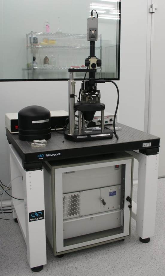
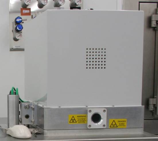
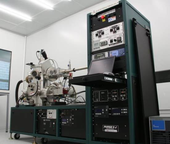
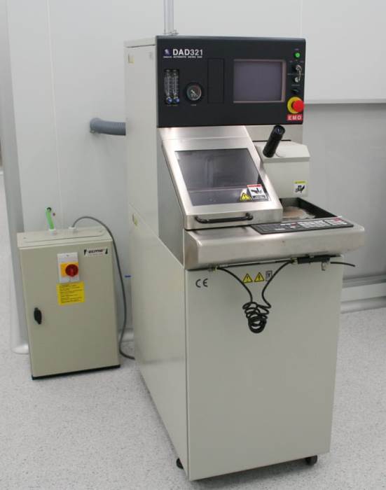
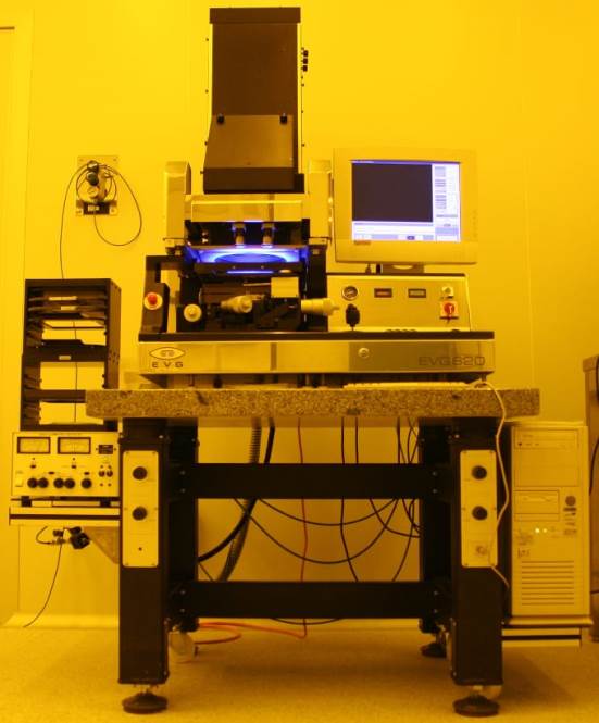
Singular equipment
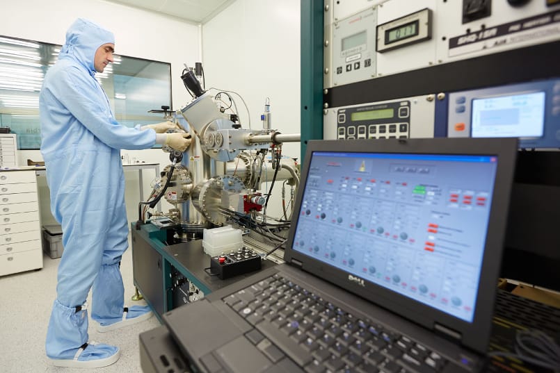
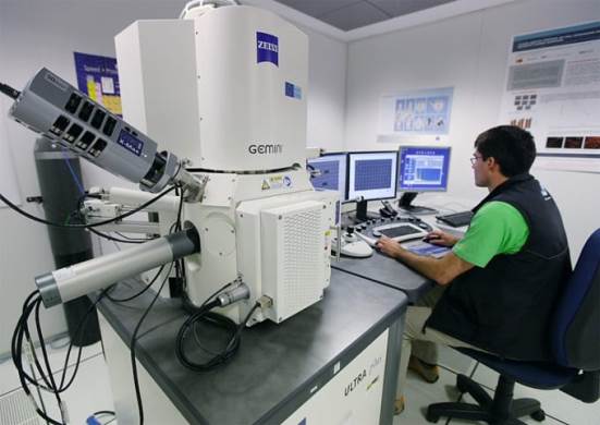
- Scanning electronic microscope (SEM)
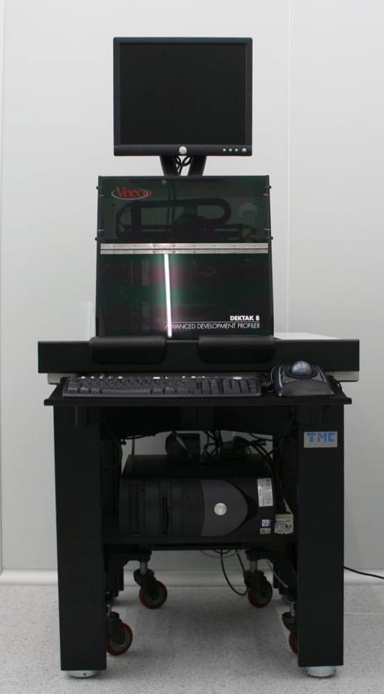
- Mechanical profilometer
- Nanoimprinting/hot embossing equipment
- Atomic force microscope
- DRIE (Deep Reactive Ion Etching) equipment
- E-BEAM deposition
- Cutting tool
- Mask aligners
Case studies
Partners network
- Universidad de Cantabria (UC)
- Universitat d´ Alacant (UA)
- Proteomika
- Instituto de Microelectrónica de Madrid (CNM – CSIC)
- IDIVAL – Instituto de investigación sanitaria de Valdecilla
Scientific excellence
- Dispositivo y método para la detección de biomarcadores
- Biosensing for disease monitoring: metallic nanohole array plasmonic sensors based on scalable nanofabrication techniques
- Dispositivo para la detección de una única molécula en situación de nanoconfinamiento y en régimen dinámico, procedimiento de fabricación y uso
- Surface plasmon resonance immunoassay for the detection of the TNF alpha biomarker in human serum
- Thermal-nanoimprint lithography for perylenediimide-based distributed feedback laser fabrication,
- Real-Time Label-Free Surface Plasmon Resonance Biosensing with Gold Nanohole Arrays Fabricated by Nanoimprint Lithography
- Improved performance of perylenediimide-based lasers
- Perylenediimide-based distributed feedback lasers with holographic relief gratings on dichromated gelatine