
Lithography
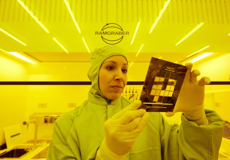
Lithography is the process by which a design consistent with a determined geometric pattern is transferred to a substrate, in such a way that this substrate is structured on a micro or nanoscale.
Nanoimprinting lithography
Hot embossing/nanoimprinting lithography enables structuring by both discontinuous and continuous methods thermoplastic polymers either deposited as a fine layer on a substrate. In the latter case it enables the replication of the original mould (master) or its inverse, by combining the technique with processes of etching or deposition.
Employing these processes, resolutions within the range of the master can be obtained, including structures falling within a range of tenths of nanometers.
Ultraviolet (UV) lithography
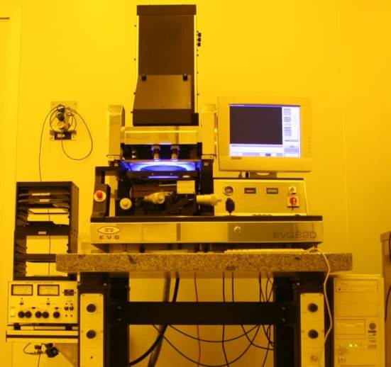
The ultraviolet photolithography aligner enables carrying out photolithographic processes on flat substrates of up to 6 inches diameter (which may be extended to larger surfaces), for manufacturing microstructures (resolution of up to 1 µm) that can be employed in sensor systems, microfluidics, soft lithographic and other systems.
The process is compatible with the EVG 501 anodic bonding equipment and enables the alignment of the substrate on both sides.
Characteristics of the lithography
- Nanoimprinting lithography enables the fast manufacture of polymeric prototypes.
- Nanoimprinting lithography enables the replication of stamps with nanometric patterns.
- The micro and nanostructured substrates manufactured using lithography can be employed for highly diverse applications (optical and photonic, biotechnology, sensor systems, obtaining superhydrophobic surfaces, decorative finishes, anti-counterfeiting designs, and so on).
Industrial sectors

Singular equipment
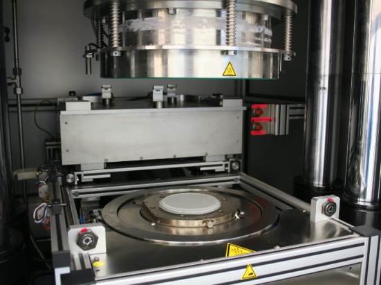
- Jenoptik HEX 03 hot embossing/lithography nanoimprint system
- EVG 620 ultraviolet photolithography aligner
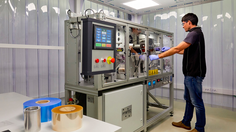
- Continuous stamping system with nanoimprinting lithography
Case studies
- Linear and angular encoders
- Patterning of proteins and cells
- Superhydrophobic and self-cleaning surfaces
Partners network
- Paul Scherrer Institut
- Universidade do Minho
- Institut Català de Nanociència i Nanotecnologia
- Danmarks Tekniske Universitet
- Instituto de Microelectrónica de Barcelona
Scientific excellence
- Dispositivo para la detección de una única molécula en situación de nanoconfinamiento y en régimen dinámico, procedimiento de fabricación y uso
- Biosensing for disease monitoring: metallic nanohole array plasmonic sensors based on scalable nanofabrication techniques
- Artificial dermis, artificial skin, methods for their preparation and their uses
- Dispositivo y método para la detección de biomarcadores
- Thermal-nanoimprint lithography for perylenediimide-based distributed feedback laser fabrication
- Perylenediimide-based distributed feedback lasers with holographic relief gratings on dichromated gelatin
- Improved performance of perylenediimide-based lasers
- Preliminary study on different technological tools and polymeric materials towards superhydrophobic surfaces for automotive applications
- Real-Time Label-Free Surface Plasmon Resonance Biosensing with Gold Nanohole Arrays Fabricated by Nanoimprint Lithography