
Bonding
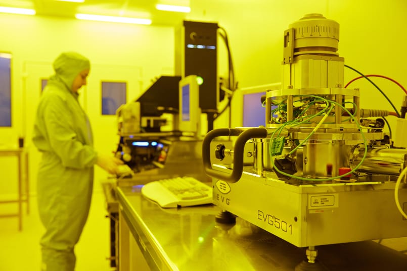
Bonding processes, particularly those involving silicon and glass, are commonly employed in electronics and in microfluidic applications.
TEKNIKER carries out anodic bonding processes with silicon and glass (it is also possible to bond metal and glass) and bonding by silicon-silicon fusion. It is also possible to undertake other kinds of bonding processes such as glass frit, eutectic, diffusion, adhesive, and so on, as well as other thermal processes.
Voltages of up to 2000 V and temperatures of up to 550ºC can be employed, enabling working with substrates of up to 4 inches diameter. Compatibility with an ultraviolet aligner is also possible. TEKNIKER is especially skilled in the sealing of microfluidic devices.
The most outstanding characteristics of this technology are the following:
- Resistant and irreversible bonding
- Compatibility with aligner
- Variety of bonding processes
Singular equipment
Case studies
Scientific excellence
- Dispositivo para la detección de una única molécula en situación de nanoconfinamiento y en régimen dinámico, procedimiento de fabricación y uso
- Design and fabrication using nanoimprint lithography of a nanofluidic device for DNA stretching applications
- DNA analysis by single molecule stretching in nanofluidic biochips